Achieving EMI agency compliance for a medical device
Client – Fortune 500 medical device manufacturer
Capabilities Demonstrated
Electromagnetic Interference (EMI) – Root Cause Analysis and Countermeasures
Challenge
The Fortune 500 client approached AppliedLogix with an urgent request to critically assess their production intent imaging subsystem design that was failing EMI compliance testing for radiated emissions levels. The failing subsystem was a vital element within a new product platform they were developing and readying for launch.
Their internal engineering staff along with the subcontractor’s engineering team (who designed the imaging subsystem) had worked for many months but were struggling to identify and remedy the design shortfalls causing the EMI emissions. The subcontractor had attempted several PCBA design spin iterations, all without success. The client team and subcontractor were both under intense pressure from senior management to solve the problems ASAP and get the product platform certified and released into full production.
Solution
AppliedLogix immediately accepted the challenge and defined a step-wise plan of action:
- Gather and review all EMI testing data collected to date and correlate the failing frequencies with specific circuit components and interconnects.
- Critically assess (from an EMC perspective) the subsystem design including the schematics, PCB layouts, and interconnect cabling.
- Develop one or more root cause hypothesis for the sources of the excessive emissions levels.
- Gather additional quantitative data, e.g., near-field probing with spectrum analyzer, as needed to better quantify and support (or disprove) the working hypothesis.
- Propose a ranked list of potential countermeasures and design updates to mitigate the emissions problems.
Within 1 week of initiating the subsystem analysis work, AppliedLogix produced an initial findings summary report that correctly and precisely identified the root cause and source of the radiated emissions.
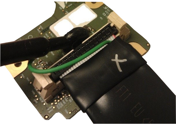
Near-field probing the sensor board at the ribbon cable connection
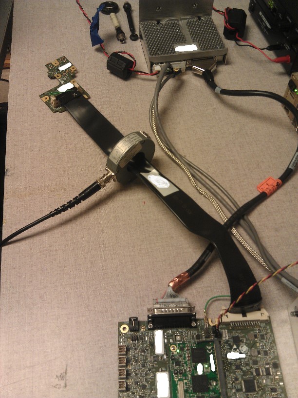
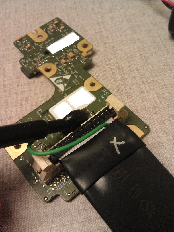
Measuring common-mode noise current on the ribbon cable shield
The primary root cause issues identified included:
- The number of signal return pins allocated within a ribbon cable interconnect between the DSP-based control board and the CCD sensor board was found to be inadequate (with a 9:1 ratio of digital IO pins to signal return pins). The lack of a sufficient allocation of signal return pins created both common-impedance coupling issues and generated an unwanted ground bounce voltage within the ribbon cable and the attached sensor board ground plane structures.
- Further, the digital IO within this compromised ribbon cable interconnect included several CCD clock signals (driven by a Spartan-6 FPGA). The drive strength (24 mA) and fast slew rate settings defined by the subcontractor exacerbated the magnitude of the induced ground bounce voltage.
- Secondary issues (for both the control board and the sensor board) – the PCB stackup, via-to-SMD-pad construction, signal trace routing and signal return path management were far from optimum.
Specific design updates were specified within the final report to reduce the signal to signal crosstalk levels as well as reduce the common mode noise floor levels on these PCBAs.
Benefits
- In ~ 2 weeks, AppliedLogix was able to jump in, apply its unique EMC analysis expertise, and deliver critical root cause analysis results along with the specific countermeasures to apply.
- The client was able to move forward rapidly with applying the recommended changes to the imaging subsystem.
- With the changes in-place, the EMI radiated emissions were greatly reduced and the entire product passed Agency certification testing.