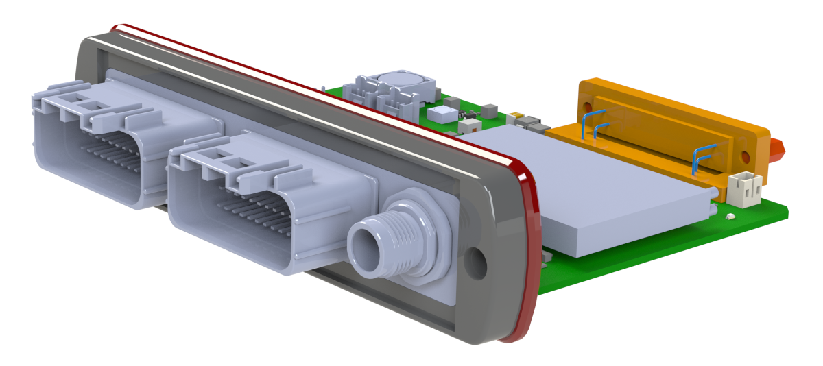
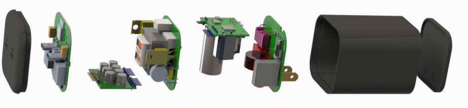
PCB Layout Services
Over 1,000 printed circuit board layouts completed
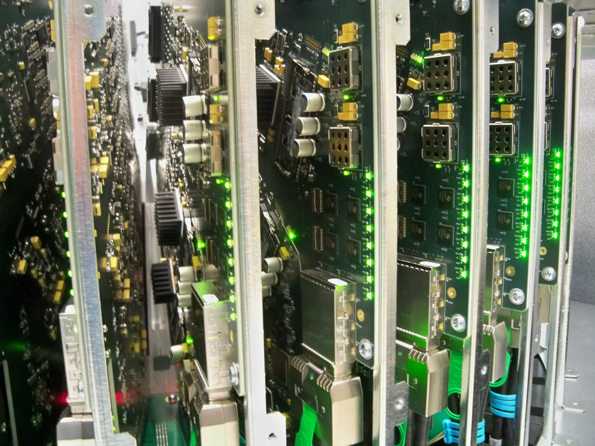
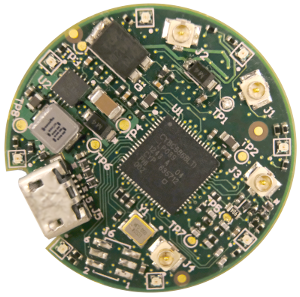
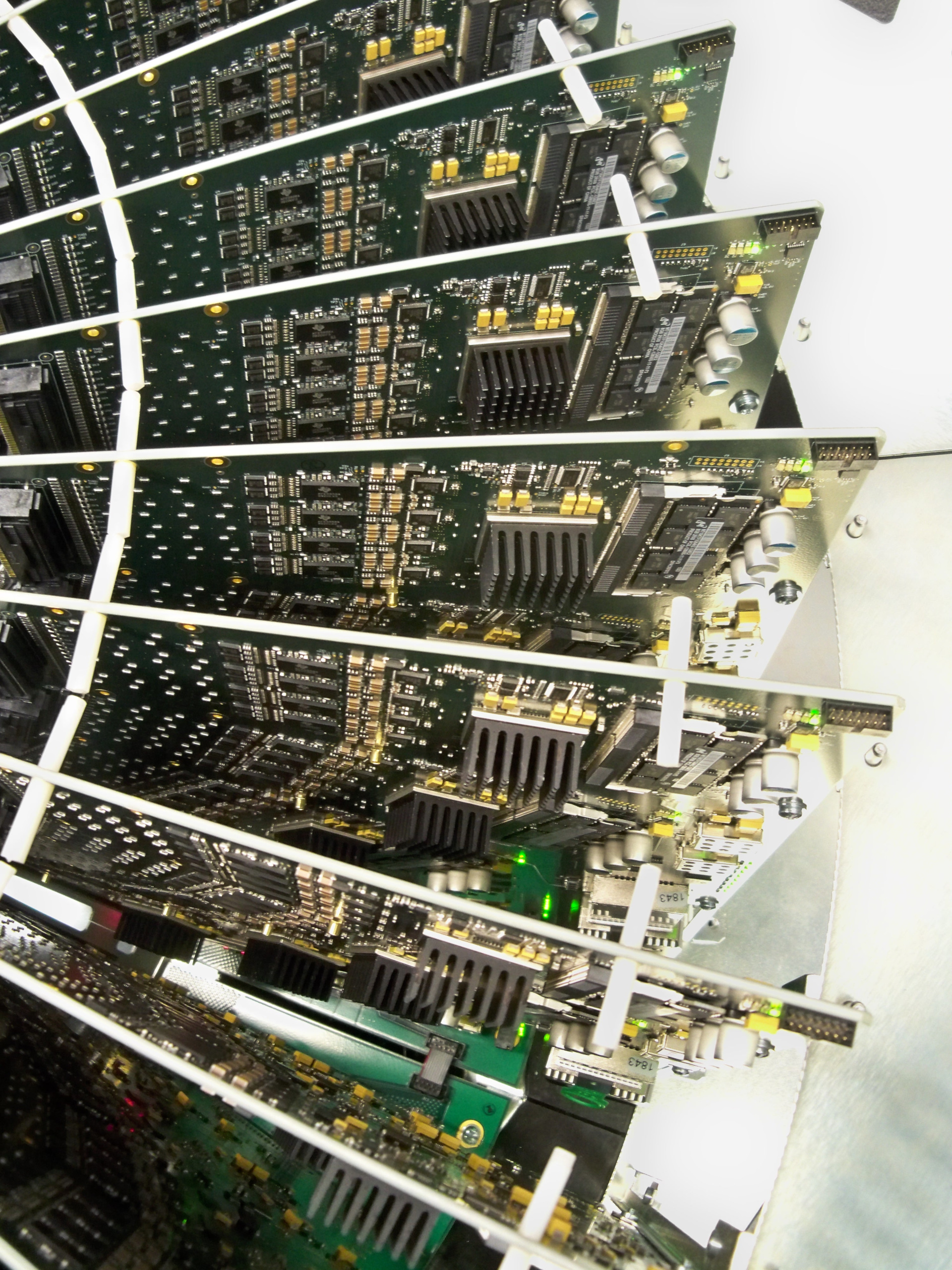
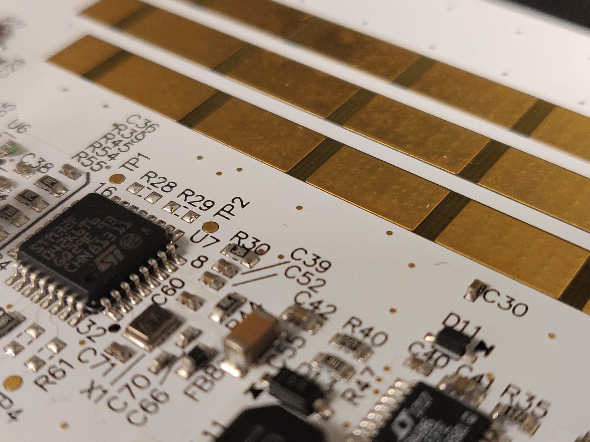
- High-speed PCB layout (FPGA, high-speed serial, impedance matching)
2 to 24+ layers, controlled impedance
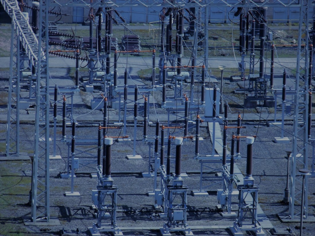
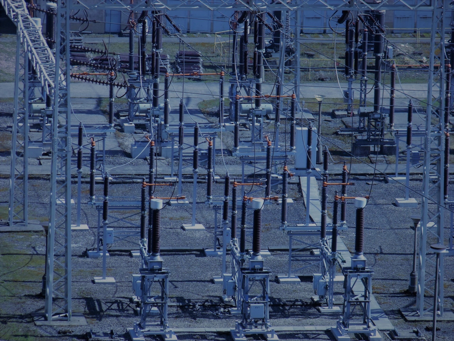
- Printed circuit board layout for improved electromagnetic compatibility (EMC)
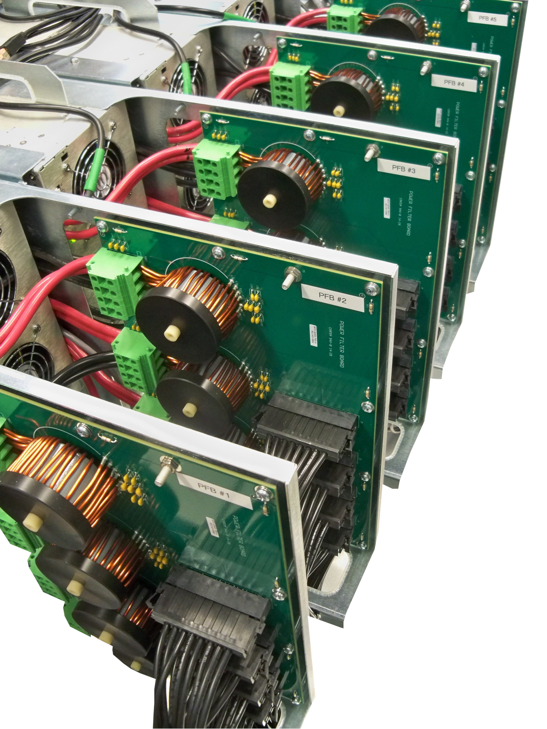
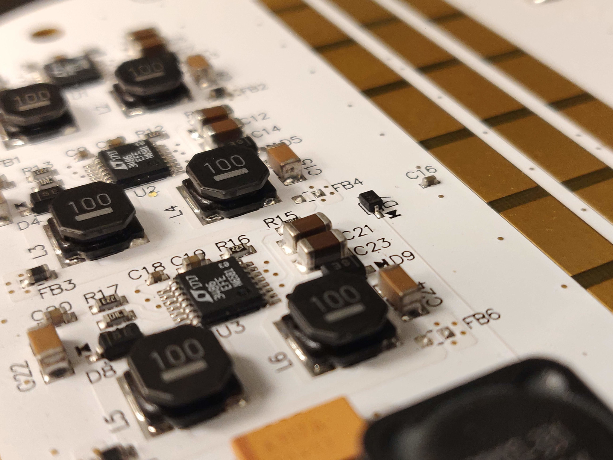
- Analog layout expertise – from low noise / high-gain to high power switch-mode circuitry
Capabilities
- IPC-certified PCB Designers with 90+ years of expertise
- Altium Designer CAE Tools
- Every design – 100% hand-routed with customized/proprietary routing constraints
- IPC Class 2 or Class 3 compliance
- Via-in-pad, blind & buried via, HDI micro-via, via modeling, and via-stub management
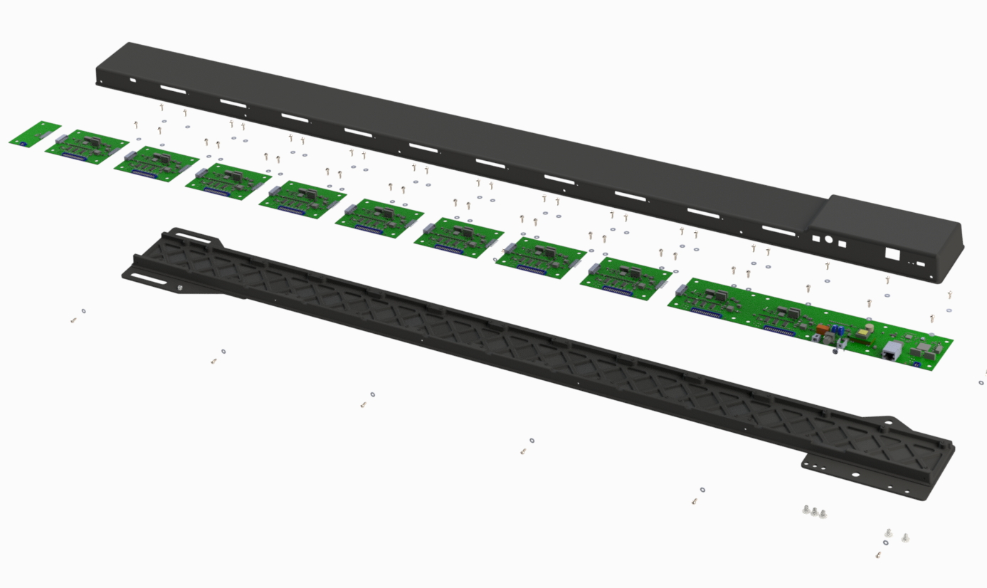
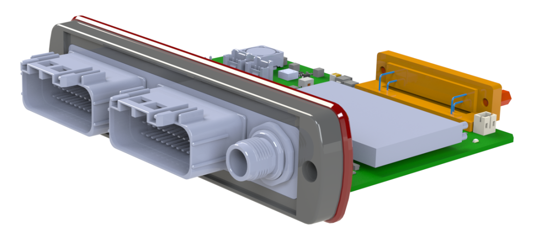
- Rigid, flex, and rigid-flex substrates
- High power density DC-DC switcher expertise
- High voltage – up to 5,000 VDC creepage and clearance
- Full 3D modeling – STEP file generation
- CAM / DFM review
- Mechanical design support
- Thermal Analysis
- DFM / DFT / DFA optimizations
- Low noise precision analog
- Signal integrity and EMC optimizations– pre and post route analysis with Mentor Hyperlynx GHZ tools
- Crosstalk minimization driven through routing constraints and verified with post-route analysis with Hyperlynx Boardsim.
- 10 to 20 GHZ+ FPGA SERDES channels
- Low loss dielectrics, spread-glass options
- S-Parameter extraction for insertion loss and return loss modeling
- IBIS-AMI based channel analysis
- DDR2/DDR3/DDR4 memory subsystems (including DDR4 @ 1.2 GHz)
- Power Integrity – low inductance PDN design
- BGA via-field DC drop simulation
- Spreadsheet-based AC analysis
Circuit Board Layout Case Studies


What a few of our clients have to say
…There are many high power / high current PWM channels and the critical low noise signals are perfectly quiet, there is no discernible noise at all. The layout is extraordinary – well done AppliedLogix!
Thank you for all the help that you have shared with the team. Much of our layout success can be attributed to the wealth of knowledge and experience that you’ve shared with us over the past couple quarters
AppliedLogix has earned special recognition… the driving force behind the architecture specification, detailed design, PWB layout, and prototype design validation of this high-performance image path subsystem.
The new layout for the AVDD power planes is excellent – great job of maximizing the clearance to critical input nodes… Very well thought out and executed… You should be proud of this work! Ship it!